Research Highlights from The 2D Quantum Materials Convergence Technology Laboratory
Xiaoxu Zhao,and Kian Ping Loh* et al., NATURE (2020) doi.org/10.1038/s41586-020-2241-9 |
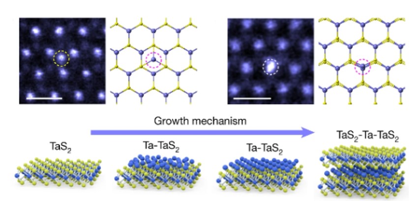
Engineering covalently bonded 2D layered materials by self-intercalationTwo-dimensional (2D) materialsoffer a unique platform from which to explore the physics of topology and many-body phenomena. New properties can be generated by filling the van der Waals gap of 2D materials with intercalants; however, post-growth intercalation has usually been limited to alkali metals. Here we show that the self-intercalation of native atoms into bilayer transition metal dichalcogenides during growth generates a class of ultrathin, covalently bonded materials, which we name ic-2D. The stoichiometry of these materials is defined by periodic occupancy patterns of the octahedral vacancy sites in the van der Waals gap, and their properties can be tuned by varying the coverage and the spatial arrangement of the filled sites. By performing growth under high metal chemical potential we can access a range of tantalum-intercalated TaS(Se)y, including 25% Ta-intercalated Ta9S16, 33.3% Ta-intercalated Ta7S12, 50% Ta-intercalated Ta10S16, 66.7% Ta-intercalated Ta8Se12 (which forms a Kagome lattice) and 100% Ta-intercalated Ta9Se12. Ferromagnetic order was detected in some of these intercalated phases. We also demonstrate that self-intercalated V11S16, In11Se16 and FexTey can be grown under metal-rich conditions. Our work establishes self-intercalation as an approach through which to grow a new class of 2D materials with stoichiometry- or composition-dependent properties. |
||
|---|---|---|---|
Peng Song,and Kian Ping Loh* et al., NATURE MATERIALS (2020) doi.org/10.1038/s41563-019-0600-4 |
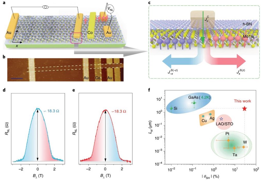
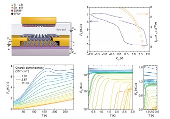
Coexistence of large conventional and planar spin Hall effect with long spin diffusion length in a low-symmetry semimetal at room temperatureThe spin Hall effect (SHE) is usually observed as a bulk effect in high-symmetry crystals with substantial spin–orbit coupling (SOC), where the symmetric spin–orbit field imposes a widely encountered trade-off between spin Hall angle (θSH) and spin diffusion length (Lsf), and spin polarization, spin current and charge current are constrained to be mutually orthogonal. Here, we report a large θSH of 0.32 accompanied by a long Lsf of 2.2 μm at room temperature in a low-symmetry few-layered semimetal MoTe2, thus identifying it as an excellent candidate for simultaneous spin generation, transport and detection. In addition, we report that longitudinal spin current with out-of-plane polarization can be generated by both transverse and vertical charge current, due to the conventional and a newly observed planar SHE, respectively. Our study suggests that manipulation of crystalline symmetries and strong SOC opens access to new charge-spin interconversion configurations and spin–orbit torques for spintronic applications. |
||
|
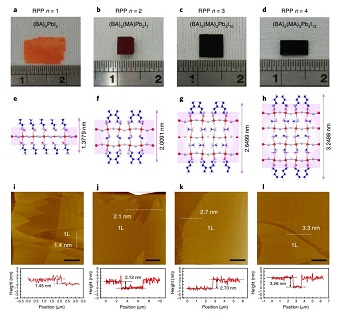
Molecularly thin two-dimensional hybrid perovskites with tunable optoelectronic properties due to reversible surface relaxationDue to their layered structure, two-dimensional Ruddlesden–Popper perovskites (RPPs), composed of multiple organic/inorganic quantum wells, can in principle be exfoliated down to few and single layers. These molecularly thin layers are expected to present unique properties with respect to the bulk counterpart, due to increased lattice deformations caused by interface strain. Here, we have synthesized centimetre-sized, pure-phase single-crystal RPP perovskites (CH3(CH2)3NH3)2(CH3NH3)n−1PbnI3n+1 (n=1–4) from which single quantum well layers have been exfoliated. We observed a reversible shift in excitonic energies induced by laser annealing on exfoliated layers encapsulated by hexagonal boron nitride. Moreover, a highly efficient photodetector was fabricated using a molecularly thin n=4 RPP crystal, showing a photogain of 105 and an internal quantum efficiency of ~34%. Our results suggest that, thanks to their dynamic structure, atomically thin perovskites enable an additional degree of control for the bandgap engineering of these materials. |
||
Yan Peng Liu and Kian Ping Loh et. al., Nature Nanotechnology, 2018, DOI: 10.1038/s41565-018-0178-z |
Tailoring sample-wide pseudo-magnetic fields on a graphene–black phosphorus heterostructure
Spatially tailored pseudo-magnetic fields (PMFs) can give rise to pseudo-Landau levels and the valley Hall effect in graphene. At an experimental level, it is highly challenging to create the specific strain texture that can generate PMFs over large areas. Here, we report that superposing graphene on multilayer black phosphorus creates shear-strained superlattices that generate a PMF over an entire graphene–black phosphorus heterostructure with edge size of tens of micrometres. The PMF is intertwined with the spatial period of the moiré pattern, and its spatial distribution and intensity can be modified by changing the relative orientation of the two materials. We show that the emerging pseudo-Landau levels influence the transport properties of graphene–black phosphorus field-effect transistor devices with Hall bar geometry. The application of an external magnetic field allows us to enhance or reduce the effective field depending on the valley polarization with the prospect of developing a valley filter. |
||
Xing Li and Kian Ping Loh et. al. Nature Communications 9, Article number: 2335 (2018) |
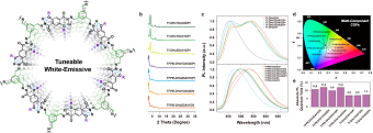
Tuneable near white-emissive two-dimensional covalent organic frameworks
Most two-dimensional (2D) covalent organic frameworks (COFs) are non-fluorescent in the solid state even when they are constructed from emissive building blocks. The fluorescence quenching is usually attributed to non-irradiative rotation-related or π–π stacking-caused thermal energy dissipation process. Currently there is a lack of guiding principle on how to design fluorescent, solid-state material made of COF. Herein, we demonstrate that the eclipsed stacking structure of 2D COFs can be used to turn on, and tune, the solid-state photoluminescence from non-emissive building blocks by the restriction of intramolecular bond rotation via intralayer and interlayer hydrogen bonds among highly organized layers in the eclipse-stacked COFs. Our COFs serve as a platform whereby the size of the conjugated linkers and side-chain functionalities can be varied, rendering the emission colour-tuneable from blue to yellow and even white. This work provides a guide to design new solid-state emitters using COFs. |
||
|
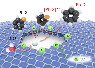
Controllable deuteration of halogenated compounds by photocatalytic D2O splitting
Deuterium labeling is of great value in organic synthesis and the pharmaceutical industry. However, the state-of-the-art C–H/C–D exchange using noble metal catalysts or strong bases/acids suffers from poor functional group tolerances, poor selectivity and lack of scope for generating molecular complexity. Herein, we demonstrate the deuteration of halides using heavy water as the deuteration reagent and porous CdSe nanosheets as the catalyst. The deuteration mechanism involves the generation of highly active carbon and deuterium radicals via photoinduced electron transfer from CdSe to the substrates, followed by tandem radicals coupling process, which is mechanistically distinct from the traditional methods involving deuterium cations or anions. Our deuteration strategy shows better selectivity and functional group tolerances than current C–H/C–D exchange methods. Extending the synthetic scope, deuterated boronic acids, halides, alkynes, and aldehydes can be used as synthons in Suzuki coupling, Click reaction, C–H bond insertion reaction etc. for the synthesis of complex deuterated molecules. |
||
|
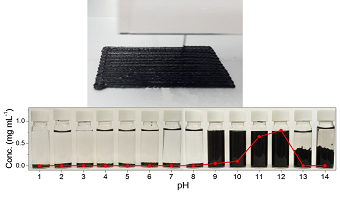
A non-dispersion strategy for large-scale production of ultra-high concentration graphene slurries in water
It is difficult to achieve high efficiency production of hydrophobic graphene by liquid phase exfoliation due to its poor dispersibility and the tendency of graphene sheets to undergo π−π stacking. Here, we report a water-phase, non-dispersion exfoliation method to produce highly crystalline graphene flakes, which can be stored in the form of a concentrated slurry (50 mg mL−1) or filter cake for months without the risk of re-stacking. The as-exfoliated graphene slurry can be directly used for 3D printing, as well as fabricating conductive graphene aerogels and graphene−polymer composites, thus avoiding the use of copious quantities of organic solvents and lowering the manufacturing cost. This non-dispersion strategy paves the way for the cost-effective and environmentally friendly production of graphene-based materials. |
||
|
Tuning magnetoresistance in molybdenum disulphide and graphene using a molecular spin transition
Coupling spins of molecular magnets to two-dimensional (2D) materials provides a framework to manipulate the magneto-conductance of 2D materials. However, with most molecules, the spin coupling is usually weak and devices fabricated from these require operation at low temperatures, which prevents practical applications. Here, we demonstrate field-effect transistors based on the coupling of a magnetic molecule quinoidal dithienyl perylenequinodimethane (QDTP) to 2D materials. Uniquely, QDTP switches from a spin-singlet state at low temperature to a spin-triplet state above 370 K, and the spin transition can be electrically transduced by both graphene and molybdenum disulphide. Graphene-QDTP shows hole-doping and a large positive magnetoresistance ( ~ 50%), while molybdenum disulphide-QDTP demonstrates electron-doping and a switch to large negative magnetoresistance ( ~ 100%) above the magnetic transition. Our work shows the promise of spin detection at high temperature by coupling 2D materials and molecular magnets. |
||
Chengxin Peng and Kian Ping Loh* et. al. NATURE ENERGY, 2, 17074 (2017) |
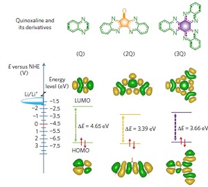
Reversible multi-electron redox chemistry of π-conjugated N-containing heteroaromatic molecule-based organic cathodes
Even though organic molecules with well-designed functional groups can be programmed to have high electron density per unit mass, their poor electrical conductivity and low cycle stability limit their applications in batteries. A team led by Prof Loh Kian Ping report the facile synthesis of π-conjugated quinoxaline-based heteroaromatic molecules (3Q) by condensation of cyclic carbonyl molecules with o-phenylenediamine. 3Q features a number of electron-deficient pyrazine sites, where multiple redox reactions take place, which was probed using in-situ 15N and 13C solid state Nuclear Magnetic Resonance. When hybridized with graphene and coupled with an ether-based electrolyte, an organic cathode based on 3Q molecules displays a discharge capacity of 395 mAh g−1 at 400 mA g−1 (1C) in the voltage range of 1.2–3.9 V and a nearly 70% capacity retention after 10,000 cycles at 8 A g−1. This work is important in demonstrating that heteroaromatic molecules with multiple redox sites are promising in developing high-energy-density, long-cycle-life organic rechargeable batteries. |
||
|
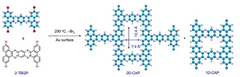
A Two-dimensional Conjugated Aromatic Polymer via C-C Coupling Reaction
The synthesis of crystalline two-dimensional (2D) conjugated polymers with well-defined repeating units and porosity presents complex challenges to synthetic chemists. Here we report a crystalline 2D conjugated aromatic polymer (2D-CAP) synthesized via C-C coupling reactions. Scanning tunneling microscopy study reveals that C-C coupling among 2-TBQP monomers on Au(111) generates 2D-CAP and its one-dimensional analogue. Interestingly, the pre-arranged 2-TBQP monomers in its crystals undergo C-C coupling driven endogenous solid-state polymerization to produce crystalline 2D-CAP. 2D-CAP can be mechanically exfoliated into micrometer-sized lamellar sheets with a thickness of 1nm. Gas sorption isothermal measurements of bulk 2D-CAP reveal a dominant pore size of ~0.6 nm, indicating uniform open channels from the eclipsed stacking of 2D-CAP sheets. 2D-CAP allows fast charge/discharge of sodium ions when employed as an organic anode in an ambient temperature sodium cell. It gives a reversible capacity of 114 mAh g-1 at a high current density of 5.0 A g-1 and retains 70% of its capacity after 7700 cycles. |
||
Zhongxin Chen, Kai Leng and Kian Ping Loh* et. al. NATURE COMMUNICATIONS, 8, 14548 (2017). |
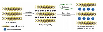
Interface confined hydrogen evolution reaction in zero valent metal nanoparticles-intercalated molybdenum disulfide
Interface confined reactions, which can modulate the bonding of reactants with catalytic centres and influence the rate of the mass transport from bulk solution, have emerged as a viable strategy for achieving highly stable and selective catalysis. Here we demonstrate that 1T′-enriched lithiated molybdenum disulfide is a highly powerful reducing agent, which can be exploited for the in-situ reduction of metal ions within the inner planes of lithiated molybdenum disulfide to form a zero valent metal-intercalated molybdenum disulfide. The confinement of platinum nanoparticles within the molybdenum disulfide layered structure leads to enhanced hydrogen evolution reaction activity and stability compared to catalysts dispersed on carbon support. In particular, the inner platinum surface is accessible to charged species like proton and metal ions, while blocking poisoning by larger sized pollutants or neutral molecules. This points a way forward for using bulk intercalated compounds for energy related applications. |
||
Hai Xu and Kian Ping Loh* et. al. NATURE COMMUNICATIONS, 7, 12904 (2016) |
|
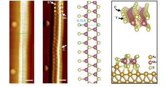
Oscillating edge states in one-dimensional MoS2 nanowires
Reducing the dimensionality of transition metal dichalcogenides to one dimension opens it to structural and electronic modulation related to charge density wave and quantum correlation effects arising from edge states. The greater flexibility of a molecular scale nanowire allows a strain-imposing substrate to exert structural and electronic modulation on it, leading to an interplay between the curvature-induced influences and intrinsic ground-state topology. Herein, the templated growth of MoS2 nanowire arrays consisting of the smallest stoichiometric MoS2building blocks is investigated using scanning tunnelling microscopy and non-contact atomic force microscopy. Our results show that lattice strain imposed on a nanowire causes the energy of the edge states to oscillate periodically along its length in phase with the period of the substrate topographical modulation. This periodic oscillation vanishes when individual MoS2 nanowires join to form a wider nanoribbon, revealing that the strain-induced modulation depends on in-plane rigidity, which increases with system size. |
|
|
Controlling many-body states by the electric-field effect in a two-dimensional material
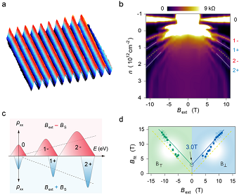
By studying 1T-TiSe2 single crystals with thicknesses of 10 nanometres or less, encapsulated in two-dimensional layers of hexagonal boron nitride, we achieve unprecedented control over the CDW transition temperature (tuned from 170 kelvin to 40 kelvin), and over the superconductivity transition temperature (tuned from a quantum critical point at 0 kelvin up to 3 kelvin). Electrically driving TiSe2 over different ordered electronic phases allows us to study the details of the phase transitions between many-body states. Observations of periodic oscillations of magnetoresistance induced by the Little–Parks effect show that the appearance of superconductivity is directly correlated with the spatial texturing of the amplitude and phase of the superconductivity order parameter, corresponding to a two-dimensional matrix of superconductivity. We infer that this superconductivity matrix is supported by a matrix of incommensurate CDW states embedded in the commensurate CDW states. Our results show that spatially modulated electronic states are fundamental to the appearance of two-dimensional superconductivity. |
||
|
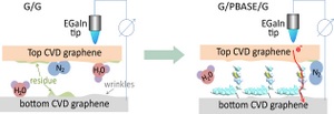
Giant Enhancement in Vertical Conductivity of Stacked CVD Graphene sheets by Self-assembled Molecular Layers
Layer-by-layer stacked chemical vapor deposition graphene films find applications as transparent and conductive electrodes in solar cells, organic light-emitting diodes and touch panels. Common to lamellar type systems with anisotropic electron delocalization, the plane-to-plane (vertical) conductivity in such systems is several orders lower than its in-plane conductivity. The poor electronic coupling between the planes is due to the presence of transfer-process organic residues and trapped air pocket in wrinkles. Here, we show the plane-to-plane tunneling conductivity of stacked CVD graphene layers can be improved significantly by inserting 1-pyrenebutyric acid N-hydroxysuccinimide ester between the graphene layers. The 6 orders of magnitude increase in plane-to-plane conductivity is due to hole doping, orbital hybridization, planarization and the exclusion of polymer residues. Our results highlight the importance of interfacial modification for enhancing the performance of LBL stacked CVD graphene films, which should be applicable to other types of stacked two dimensional films. |
||
|
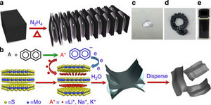
High Yield Exfoliation of Two-dimensional Chalcogenides Using Sodium Naphthalenide
Transition-metal dichalcogenides like molybdenum disulphide have attracted great interest as two-dimensional materials beyond graphene due to their unique electronic and optical properties. Solution-phase processes can be a viable method for producing printable single-layer chalcogenides. Molybdenum disulphide can be exfoliated into monolayer flakes using organolithium reduction chemistry; unfortunately, the method is hampered by low yield, submicron flake size and long lithiation time. Here we report a high-yield exfoliation process using lithium, potassium and sodium naphthalenide where an intermediate ternary LixMXn crystalline phase (X=selenium, sulphur, and so on) is produced. Using a two-step expansion and intercalation method, we produce high-quality single-layer molybdenum disulphide sheets with unprecedentedly large flake size, that is up to 400 μm2. Single-layer dichalcogenide inks prepared by this method may be directly inkjet-printed on a wide range of substrates. |
||
|
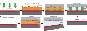
Face-to-face Transfer of Wafer-scale Graphene Films
High-fidelity transfer or direct growth of high-quality graphene films on arbitrary substrates is needed to enable wide-ranging applications in photonics or electronics, which include devices such as optoelectronic modulators, transistors, on-chip biosensors and tunnelling barriers. The direct growth of graphene film on an insulating substrate, such as a SiO2/Si wafer, would be useful for this purpose, but current research efforts remain grounded at the proof-of-concept stage, where only discontinuous, nanometre-sized islands can be obtained. Here we develop a face-to-face transfer method for wafer-scale graphene films that is so far the only known way to accomplish both the growth and transfer steps on one wafer. This spontaneous transfer method relies on nascent gas bubbles and capillary bridges between the graphene film and the underlying substrate during etching of the metal catalyst, which is analogous to the method used by tree frogs to remain attached to submerged leaves. In contrast to the previous wet or dry transfer results, the face-to-face transfer does not have to be done by hand and is compatible with any size and shape of substrate; this approach also enjoys the benefit of a much reduced density of transfer defects compared with the conventional transfer method. Most importantly, the direct growth and spontaneous attachment of graphene on the underlying substrate is amenable to batch processing in a semiconductor production line, and thus will speed up the technological application of graphene. |
||
|
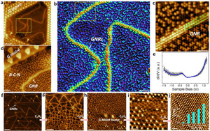
Order–disorder Transition in a Two-dimensional Boron–carbon–nitride Alloy
Two-dimensional boron–carbon–nitride materials exhibit a spectrum of electronic properties ranging from insulating to semimetallic, depending on their composition and geometry. Detailed experimental insights into the phase separation and ordering in such alloy are currently lacking. Here we report the mixing and demixing of boron–nitrogen and carbon phases on ruthenium (0001) and found that energetics for such processes are modified by the metal substrate. The brick-and-mortar patchwork observed of stoichiometrically percolated hexagonal boron–carbon–nitride domains surrounded by a network of segregated graphene nanoribbons can be described within the Blume–Emery–Griffiths model applied to a honeycomb lattice. The isostructural boron nitrideand graphene assumes remarkable fluidity and can be exchanged entirely into one another by a catalytically assistant substitution. Visualizing the dynamics of phase separation at the atomic level provides the premise for enabling structural control in a two-dimensional network for broad nanotechnology applications. |
||
|
A Hydrothermal Anvil Made of Graphene Nanobubbles on Diamond
The molecular structure of superheated water trapped in the bubble was probed using vibrational spectroscopy and dynamic changes in the hydrogen bonding environment was observed. The graphene-diamond hydrothermal anvil can serve as a useful bench-top construct for investigating the dynamic chemistry of supercritical phases in fluids.
|
||
Chenliang Su, Muge Acik, Kian Ping Loh et. al.; Nature Communications 3, 1298 (2012) |
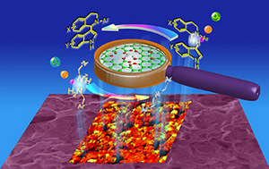
Probing the Catalytic Activity of Porous Graphene Oxide and the Origin of This Behaviour
Graphene oxide, a two-dimensional aromatic scaffold decorated by oxygen-containing functional groups, possesses rich chemical properties and may present a green alternative to precious metal catalysts. Graphene oxide-based carbocatalysis has recently been demonstrated for aerobic oxidative reactions. However, its widespread application is hindered by the need for high catalyst loadings. Here we report a simple chemical treatment that can create and enlarge the defects in graphene oxide and impart on it enhanced catalytic activities for the oxidative coupling of amines to imines (up to 98% yield at 5 wt% catalyst loading, under solvent-free, open-air conditions). This study examines the origin of the enhanced catalytic activity, which can be linked to the synergistic effect of carboxylic acid groups and unpaired electrons at the edge defects. The discovery of a simple chemical processing step to synthesize highly active graphene oxide allows the premise of industrial-scale carbocatalysis to be explored. |
||
Jiong Lu, A.H. Castro Neto & Kian Ping Loh. Nature Communications 3 (2012) 823 |
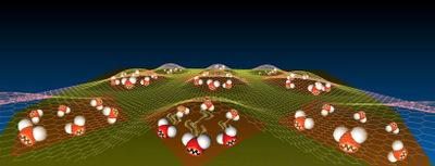
Transforming Moiré Blisters into Geometric Graphene Nano-bubbles
Strain engineering has been proposed as an alternative method for manipulating the electronic properties of graphene. However, the bottleneck for strain engineering in graphene has been the ability to control such strain patterns at the nanoscale. Here we show that high level of control can be accomplished by chemically modifying the adherence of graphene on metal. Using scanning tunnelling microscopy, the shape evolution of graphene Moiré blisters towards geometrically well-defined graphene bubbles was studied during the controlled, sub-layer oxidation of the ruthenium substrate. Understanding the dynamics of the oxidation process and defects generation on the Ru substrate allows us to control the size, shape and the density of the bubbles and its associated pseudo-magnetism. We also show that a modification of the same procedure can be used to create antidots in graphene by catalytic reaction of the same nanobubbles. |
||
|
Broadband Graphene Polarizer
Conventional polarizers can be classified into three main modes of operation: sheet polarizer using anisotropic absorption media, prism polarizer by refraction and Brewster-angle polarizer by reflection. These polarizing components are not easily integrated with photonic circuits. The in-line fibre polarizer, which relies on polarization-selective coupling between the evanescent field and birefringent crystal or metal, is a promising alternative because of its compatibility with most fibre-optic systems. Here, we demonstrate the operation of a broadband fibre polarizer based on graphene, an ultrathin two-dimensional carbon material. The out-coupled light in the telecommunication band shows a strong s-polarization effect with an extinction ratio of 27 dB. Unlike polarizers made from thin metal film, a graphene polarizer can support transverse-electric-mode surface wave propagation due to its linear dispersion of Dirac electrons. |
||
|
Transforming C60 Molecules into Graphene Quantum Dots
The fragmentation of fullerenes using ions, surface collisions or thermal effects is a complex process that typically leads to the formation of small carbon clusters of variable size. Here, we show that geometrically well-defined graphene quantum dots can be synthesized on a ruthenium surface using C60 molecules as a precursor. |
||
|
The Chemistry of Two-dimensional Layered Transition Metal Dichalcogenide Nanosheets
Ultrathin two-dimensional nanosheets of layered transition metal dichalcogenides (TMDs) are fundamentally and technologically intriguing. In contrast to the graphene sheet, they are chemically versatile. Mono- or few-layered TMDs — obtained either through exfoliation of bulk materials or bottom-up syntheses — are direct-gap semiconductors whose bandgap energy, as well as carrier type (n- or p-type), varies between compounds depending on their composition, structure and dimensionality. In this Review, we describe how the tunable electronic structure of TMDs makes them attractive for a variety of applications. They have been investigated as chemically active electrocatalysts for hydrogen evolution and hydrosulfurization, as well as electrically active materials in opto-electronics. Their morphologies and properties are also useful for energy storage applications such as electrodes for Li-ion batteries and supercapacitors. |
||
Kian Ping Loh, Qiaoliang Bao, Goki Eda & Manish Chhowalla, NATURE CHEMISTRY 2, 12, 1015-1024 (2010) |
Graphene Oxide as a Chemically Tunable Platform for Optical Applications |
||